- 您现在的位置:买卖IC网 > Sheet目录3882 > PIC16F87T-I/ML (Microchip Technology)IC MCU FLASH 4KX14 EEPROM 28QFN
162
8008H–AVR–04/11
ATtiny48/88
16.2
Register Description
16.2.1
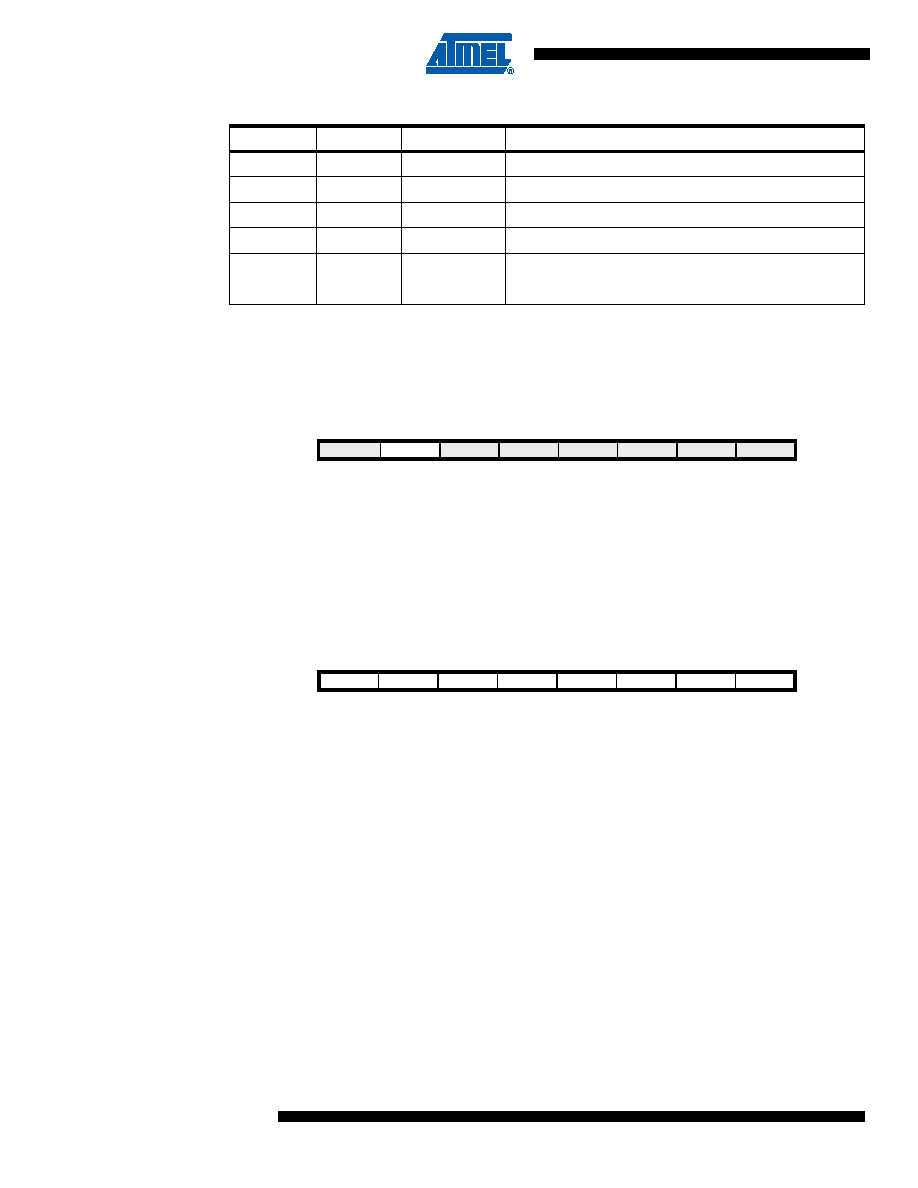
ADCSRB – ADC Control and Status Register B
Bit 6 – ACME: Analog Comparator Multiplexer Enable
When this bit is written logic one and the ADC is switched off (ADEN in ADCSRA is zero), the
ADC multiplexer selects the negative input to the Analog Comparator. When this bit is written
logic zero, AIN1 is applied to the negative input of the Analog Comparator. For a detailed
description of this bit, see “Analog Comparator Multiplexed Input” on page 161.
16.2.2
ACSR – Analog Comparator Control and Status Register
Bit 7 – ACD: Analog Comparator Disable
When this bit is written logic one, the power to the Analog Comparator is switched off. This bit
can be set at any time to turn off the Analog Comparator. This will reduce power consumption in
Active and Idle mode. When changing the ACD bit, the Analog Comparator Interrupt must be
disabled by clearing the ACIE bit in ACSR. Otherwise an interrupt can occur when the bit is
changed.
Bit 6 – ACBG: Analog Comparator Bandgap Select
When this bit is set, a fixed internal bandgap reference voltage replaces the positive input to the
Analog Comparator. When this bit is cleared, AIN0 is applied to the positive input of the Analog
Comparator. See “Internal Voltage Reference” on page 45.
Bit 5 – ACO: Analog Comparator Output
The output of the Analog Comparator is synchronized and then directly connected to ACO. The
synchronization introduces a delay of 1 – 2 clock cycles.
1
0
010
ADC2
1
0
011
ADC3
1
0
100
ADC4
1
0
101
ADC5
1
0
110
ADC6
1
0
111
ADC7
Table 16-1.
Analog Comparator Multiplexed Input (Continued)
ACME
ADEN
MUX[2:0]
Analog Comparator Negative Input
Bit
7
65432
10
–ACME
–
ADTS2
ADTS1
ADTS0
ADCSRB
Read/Write
R
R/W
R
R/W
Initial Value
0
00000
00
Bit
7
654
32
10
ACD
ACBG
ACO
ACI
ACIE
ACIC
ACIS1
ACIS0
ACSR
Read/Write
R/W
R
R/W
Initial Value
0
N/A
0
发布紧急采购,3分钟左右您将得到回复。
相关PDF资料
PIC16F87T-E/ML
IC MCU FLASH 4KX14 EEPROM 28QFN
PIC16F87-E/ML
IC MCU FLASH 4KX14 EEPROM 28QFN
PIC18LF4320-I/ML
IC MCU FLASH 4KX16 EEPROM 44QFN
PIC16F77T-I/PTG
IC MCU FLASH 8KX14 W/AD 44TQFP
PIC16LF1933-I/SO
IC PIC MCU FLASH 4K 28-SOIC
PIC16C54C-20I/SO
IC MCU OTP 512X12 18SOIC
PIC16LF726-I/SO
IC PIC MCU FLASH 8K 1.8V 28-SOIC
PIC12CE673-10/P
IC MCU OTP 1KX14 A/D&EE 8DIP
相关代理商/技术参数
PIC16F87T-I/SO
功能描述:8位微控制器 -MCU 7KB 368 RAM 16 I/O RoHS:否 制造商:Silicon Labs 核心:8051 处理器系列:C8051F39x 数据总线宽度:8 bit 最大时钟频率:50 MHz 程序存储器大小:16 KB 数据 RAM 大小:1 KB 片上 ADC:Yes 工作电源电压:1.8 V to 3.6 V 工作温度范围:- 40 C to + 105 C 封装 / 箱体:QFN-20 安装风格:SMD/SMT
PIC16F87T-I/SS
功能描述:8位微控制器 -MCU 7KB 368 RAM 16 I/O RoHS:否 制造商:Silicon Labs 核心:8051 处理器系列:C8051F39x 数据总线宽度:8 bit 最大时钟频率:50 MHz 程序存储器大小:16 KB 数据 RAM 大小:1 KB 片上 ADC:Yes 工作电源电压:1.8 V to 3.6 V 工作温度范围:- 40 C to + 105 C 封装 / 箱体:QFN-20 安装风格:SMD/SMT
PIC16F882-E/ML
功能描述:8位微控制器 -MCU 3.5KB Enh FLSH 128 RAM RoHS:否 制造商:Silicon Labs 核心:8051 处理器系列:C8051F39x 数据总线宽度:8 bit 最大时钟频率:50 MHz 程序存储器大小:16 KB 数据 RAM 大小:1 KB 片上 ADC:Yes 工作电源电压:1.8 V to 3.6 V 工作温度范围:- 40 C to + 105 C 封装 / 箱体:QFN-20 安装风格:SMD/SMT
PIC16F882-E/SO
功能描述:8位微控制器 -MCU 3.5KB Enh FLSH 128 RAM RoHS:否 制造商:Silicon Labs 核心:8051 处理器系列:C8051F39x 数据总线宽度:8 bit 最大时钟频率:50 MHz 程序存储器大小:16 KB 数据 RAM 大小:1 KB 片上 ADC:Yes 工作电源电压:1.8 V to 3.6 V 工作温度范围:- 40 C to + 105 C 封装 / 箱体:QFN-20 安装风格:SMD/SMT
PIC16F882-E/SP
功能描述:8位微控制器 -MCU 3.5KB Enh FLSH 128 RAM RoHS:否 制造商:Silicon Labs 核心:8051 处理器系列:C8051F39x 数据总线宽度:8 bit 最大时钟频率:50 MHz 程序存储器大小:16 KB 数据 RAM 大小:1 KB 片上 ADC:Yes 工作电源电压:1.8 V to 3.6 V 工作温度范围:- 40 C to + 105 C 封装 / 箱体:QFN-20 安装风格:SMD/SMT
PIC16F882-E/SS
功能描述:8位微控制器 -MCU 3.5KB Enh FLSH 128 RAM RoHS:否 制造商:Silicon Labs 核心:8051 处理器系列:C8051F39x 数据总线宽度:8 bit 最大时钟频率:50 MHz 程序存储器大小:16 KB 数据 RAM 大小:1 KB 片上 ADC:Yes 工作电源电压:1.8 V to 3.6 V 工作温度范围:- 40 C to + 105 C 封装 / 箱体:QFN-20 安装风格:SMD/SMT
PIC16F882-I/ML
功能描述:8位微控制器 -MCU 3.5KB Enh FLSH 128 RAM RoHS:否 制造商:Silicon Labs 核心:8051 处理器系列:C8051F39x 数据总线宽度:8 bit 最大时钟频率:50 MHz 程序存储器大小:16 KB 数据 RAM 大小:1 KB 片上 ADC:Yes 工作电源电压:1.8 V to 3.6 V 工作温度范围:- 40 C to + 105 C 封装 / 箱体:QFN-20 安装风格:SMD/SMT
PIC16F882-I/ML
制造商:Microchip Technology Inc 功能描述:IC 8BIT MCU PIC16F 20MHz QFN-28 制造商:Microchip Technology Inc 功能描述:IC, 8BIT MCU, PIC16F, 20MHz, QFN-28